- Text Size:


13 January 2011
Rofin demonstrate expertise in solar cell manufacturing
As a worldwide leader in development and manufacturing of industrial lasers, Rofin has over 35 years of experience in laser material processing. This knowledge and expertise has been used to develop solutions for almost any laser application in solar cell manufacturing.
Rofin used the recent EUPVSEC exhibition in Valencia, Spain to showcase just five examples from their comprehensive range of technologies, which cover thin film and c-Si technology as well as volume production and research.
Leading Laser Range for Edge Deletion
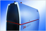 Rofin offers the world‘s broadest range of laser sources for edge deletion applications. The 800 Watt DQ x80 has in fact established itself as the top-selling laser for edge deletion of thin film cells. Furthermore, the new PowerLine L 400 covers the lower end of the spectrum. Using an optimized resonator design, which significantly increases output power, this laser source replaces the PowerLine L 300. Optimized square fibers are available for both lasers. Compared to round fibers, square fibers provide highest efficiency, machining a larger area per pulse and enabling consistent overlap of individual pulses.
New ECCI Code for Wafer Traceability Marking
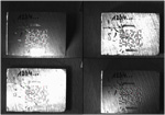 Wafer marking in solar cell manufacturing is the key to traceability and improved manufacturing processes. DataMatrix codes may be used on solar active areas but they are prone to deteriorate in the multitude of coating and etching processes. Using the new ECCI code, Rofin present a potential solution. Unlike ECC DataMatrix codes, this code is highly resistant to the changes in contrast often found on inhomogenous surfaces such as polycrystalline solar cells. As long as something is visible decoding works - even in case of contrast inversions within the marking. Additionally, ECCI code redundancy is adjustable. Marks which might be subject to heavy wear and tear can use a highly redundant coding.
Femtosecond Laser with Galvo
Rofin used the EUPVSEC event to present StarFemto, one of the first 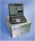 industrial-grade femtosecond lasers, combined with an optimized galvo scanner head. This setup has all of the prerequisites for R&D applications using femtosecond laser technology in photovoltaics. Femtosecond lasers hold immense potential for a new level of precision and selectivity in applications such as thin film structuring and ablation of dielectric layers. Femtosecond lasers process materials faster than energy can diffuse within the atomic lattice and therefore almost no energy diffusion to the surrounding medium takes place. Furthermore, because most of the interaction processes do not depend on linear absorption, virtually any material can be machined by the same laser beam - laser wavelength becomes marginal.
Most Versatile Lab System for Photovoltaics
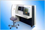 Rofin‘s PowerLine E 25 SHG is one of the few laser sources which copes with almost all applications in c-Si manufacturing, making it ideally suited to process evaluation.
Combining the PowerLine E 25 SHG with a wafer fixture, an image processing system and fine tuned, easy-to-use software, this setup provides R&D labs with the ability to easily evaluate new manufacturing methods for laser doping, SiN backside opening, laser drilling or laser edge isolation applications to name but a few.
Perfect Tool for Mass Production of Enhanced Solar Cells
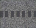 Selective opening of dielectric layers and direct laser doping currently generate a lot of interest in the crystalline solar cell manufacturing business. For both applications, the frequency-doubled PowerLine L 100 SHG has already proven to be perfectly suited in various research projects and production machines. The laser source offers optimum beam characteristics and sufficient power to achieve short cycle times and is well suited to large scale production. Green lasers with 532 nm wavelength show the desired near-surface absorption in silicon and can be equipped with a wide range of optical components and fibres. At the recent EUPVSEC event Rofin presented for the first time, it’s patent pending rectangular spot size with a top-hat beam profile.
- Contact Information
- Name: Dave MacLellan
- Email: sales@rofin-baasel.co.uk
- Website: www.rofin.co.uk