- Text Size:


4 April 2011
Lasers in thin film and c-SI photovoltaic
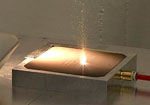
The laser has become an indispensible tool for thin-film photovoltaic module production. With most thin-film materials, the layer scribing steps required for monolithic integration cannot be performed with more flexibility and precision using any other process. This is why laser technology has been a key part of thin-film development for over two decades.
Mechanical scribing replaced wet chemical etching because the wet chemical method was too slow and also environmentally unfriendly. The wear-free laser process is much more controllable and also reduces the risk of breakage in subsequent processing. The other laser application in thin-film manufacturing is edge deletion in advance of hermetic sealing of the module. Here laser technology gradually replaced sand blasting, a dirty and environmentally questionable process, and now holds a market share of over 50% in new manufacturing facilities.
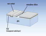 The materials processed include Transparent Conductive Oxide (TCO) layers on glass or flexible substrates, active layers on thin-film modules such as amorphous silicon (a-Si), Cadmium Telluride (CdTe) and Copper, Indium, Gallium Selenide (CIGS) and the back contact layers such as aluminium, silver, molybdenum and combinations of these.
High beam quality, which results in a large depth of focus, compensates for various material irregularities such as imperfections in flatness and thickness on large glass panels and maintains small scribe widths and constant depths. This is the reason why q-switched, diode-pumped Nd:Vanadate lasers (1064 nm or 532 nm wavelength) with short ns-pulse widths, such as Rofin‘s PowerLine SL and PowerLine L series, have become the standard laser type for both types of application.
Whereas the scribing process requires pulse energies in the range of µJ, edge deletion needs mJ laser pulses to meet production requirements of a volume production plant. Fundamental (1064 nm) and wavelengths with double frequency (532 nm) are commonly used in the production of a-Si/µ-Si, CIGS and CdS/CdTe solar cells.
Lasers and c-Si Cells - The long road to mass production
In crystalline cell manufacturing, laser technology is only considered if it contributes to reducing cost per Watts produced (c/Wp). One way that it achieves this is by streamlining the production process e.g., replacing plasma etching for edge isolation or mechanical cutting and scribing steps. Another way is through improved photovoltaic efficiency.
 Extensive research has resulted in laser-assisted manufacturing concepts for enhanced solar cells, which have been evaluated in lab production scale. However, the road to mass production is a long one, efficiency gains have to outmatch additional investment costs significantly. But intensified competition with thin-film technology currently helps some of these concepts find their way into volume production.
Laser assisted selective doping
Current mass production crystalline cells suffer from a trade-off between the desired heavy doping of the n-type silicon layer underneath the metallised contact regions and light doping between the contact fingers. The solution is selective doping of emitters, which promises efficiency gains of about one percentage point, and most new selective emitter concepts for mass production scale rely on laser material processing.
One approach is selective doping through laser ablation of dielectrics. Prior to dopant diffusion, a dielectric masking layer is generated, which is then selectively opened by lasers in the required contact areas. Therefore, the subsequent diffusion step creates different dopant concentrations on masked and non-masked areas. Direct laser doping is also a promising concept for realizing selective emitters. Through the PSG layer additional dopant Phosphor atoms are driven into the Silicon using a laser for precisely controlled, localized heat input.
Back side contact technology
Another well-explored concept for increased efficiency is back side contacted solar cells, which eliminates the otherwise necessary front side strip lines, and in this way enhances the solar-active surface. Furthermore, the entire interconnection of solar cells into modules can be achieved without any connections from the front to the rear side. Packing density increases and costs drop. The Metal Wrap Through (MWT) method requires a few dozen vias in a grid pattern on one solar cell; Emitter-Wrap-Through (EWT) cells need about 10.000. For both techniques a q-switched disc laser such as Rofin's StarDisc, provides the necessary throughput rates. The q-switched beam source provides both high power in TEM00 fundamental mode and ideal pulse widths for these applications, achieving extremely short processing times, in the range of only a few seconds, per solar cell.
With selective emitters, a well-known approach (already tested in high-efficiency cells) finds a route to mass production. It certainly won‘t be the last one, as the laser is a key technology for many tried and tested high-efficiency concepts. In addition, laser patterning and selective ablation of dielectric layers generally opens a broad field for new efficiency improvement approaches.
- Contact Information
- Name: Dave MacLellan
- Email: sales@rofin-baasel.co.uk
- Website: www.rofin-baasel.co.uk